Sputtering
Presentations | English
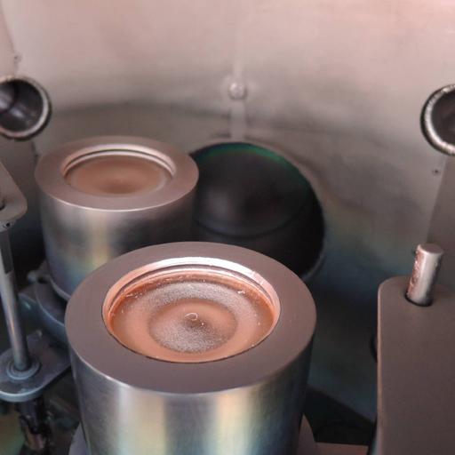
Sputtering is a phenomenon in which microscopic particles of a solid material are ejected from its surface, after the material is itself bombarded by energetic particles of a plasma or gas. Sputtering is used extensively in the semiconductor industry to deposit thin films of various materials in integrated circuit processing. Thin antireflection coatings on glass for optical applications are also deposited by sputtering. Basically the steps of sputtering process are the following: (i) the neutral gas is ionized by a external power supply, producing a glow discharge or plasma; (ii) a source (the cathode, also called the target) is bombarded in high vacuum by gas ions due to the potential drop acceleration in the cathode sheath; (iii) atoms from the target are ejected by momentum transfer and diffuse through the vacuum chamber; (iv) atoms are deposited on the substrate to be coated and form a thin film. Please find the presentation for more details.

12.75
Lumens
PPTX (51 Slides)
Sputtering
Presentations | English